Rapid Identification of the Layer Number of Large-Area Graphene on Copper
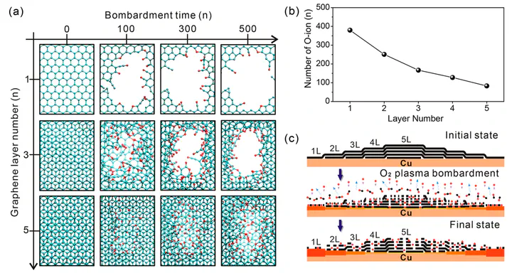 Image credit:
Abstract
Chemical vapor deposition (CVD) on Cu foils emerged as an important method for preparing high-quality and large-area graphene films for practical applications. However, to date it remains challenging to rapidly identify the structural features, especially the layer numbers, of CVD-graphene directly on Cu substrate. Herein, we report an O-2-plasma-assisted approach for identifying the coverage, wrinkles, domain size, and layer number of large-area graphene films on Cu foils by optical microscopy. The wrinkles and grain boundaries of five-layer graphene can be observed with a grayscale increment of similar to 23.4% per one graphene layer after O-2-plasma treatment for only 15 s, which allows for checking graphene on Cu foils with a sample size of 17 cm x 20 cm in a few minutes. The Raman spectroscopy and X-ray photoelectron spectroscopy presents a strong layer number dependence of both the plasma induced graphene defects and Cu oxides, which, as indicated by molecular dynamic simulation, is responsible for the improved image contrast as a result of the interaction between O-ions and graphene with different layer numbers. We expect that this O-2-plasma-assisted method would be applied to meter-scale samples if atmospheric-pressure plasma is used and therefore will be beneficial for the fast evaluation of CVD-graphene in both laboratory and industry.
Type
Publication
Chemistry of Materials
Click the Cite button above to demo the feature to enable visitors to import publication metadata into their reference management software.
Create your slides in Markdown - click the Slides button to check out the example.
Add the publication’s full text or supplementary notes here. You can use rich formatting such as including code, math, and images.